Language selection
В настоящее время портал работает - ведутся технические работы.
Catalog
Search
3936 products
View:
- Selected: 0Foreign brand
- Selected: 0By name of foreign product
- Selected: 0Item names
- Selected: 0Russian analogue
- Selected: 0Areas of use
View:
3936 products
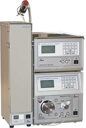
Liquid chromatograph "LUMACHROM®"
1 supp.
Technical specifications:
Operating spectral range, nm from 190 to 360
Limits of permissible absolute error of wavelength setting, nm ± 5
Detection limit of anthracene (wavelength 252 nm), ng/cm3, no more than 1
The limit of the permissible value of the relative mean square deviation of the output signal (n =5), %
of the retention
time over the peak area of 1.5
2
Limits of the permissible value of the relative change in the output signal (peak area) for 4 hours of continuous operation, % ± 5
Overall dimensions (LxWxH), mm, no more:
270x420x190
Weight, kg, not more than 9.5
Power consumption, V· A, not more than 50
Lumeks
Saint Petersburg
Produced in: Saint Petersburg
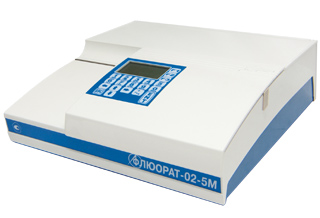
Liquid analyzer "FLUORAT®-02-5M"
1 supp.
Technical specifications:
Limit of detection of the control substance (phenol) in water, mg/dm3, no more
0,005
Measurement range of the mass concentration of the control substance (phenol) in water, mg/dm3
from 0.01 to 25 Measurement range of the directional transmission coefficient, % from 5 to 100
Limits of permissible absolute error of measurements of the directional transmission coefficient, % ± 2
Warm-up time, min, no more than 30
Continuous operation time, h, at least 8
Overall dimensions, mm, no more
than 305x320x110 Weight, kg, no more than 6.5
AC power supply:
- AC power supply voltage, V
- frequency, Hz
(220 ±22)
(50 ±1) Power consumption, In × A, no more than 36
Time to failure, h, not less than 2500
Lumeks
Saint Petersburg
Produced in: Saint Petersburg
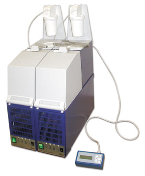
Sample preparation system – microwave mineralizer "MINOTAUR®-2"
1 supp.
Technical specifications:
Frequency of the generated magnetron radiation, MHz 2450 ±50
Number of simultaneously decomposed samples 1
The maximum volume of the processed sample, cm3 50
Maximum working pressure in the container, atm 9
Power consumption, V*A 600
The average absorbed power (W) in the reactor when heating 30 cm3 of distilled water at 100% output power level of the magnetron in the range of supply voltage from 187 to 242 V
150... 250 Average time to failure, h, not less than 2500
Average service life, years, at least 5
Overall dimensions, mm, no more than 500x450x150
Weight, kg, no more than 22
Lumeks
Saint Petersburg
Produced in: Saint Petersburg
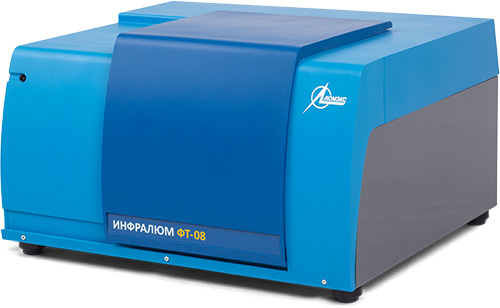
Infrared Fourier spectrometer "InfraLUM® FT-08"
1 supp.
Technical specifications:
Operating spectral range, cm-1 from 400 to 7800
Spectral resolution, cm-1, not more than 0.7
The limit of the absolute error of the wavenumber scale, cm-1 ± 0.05 Signal-to-noise ratio (RMS) for the wavenumber 2150 cm-1, determined in the range ± 50 cm-1 for a resolution of 4 cm-1 and an accumulation time of 60 s, at least 40,000 The limit of deviation of the 100% transmission line from the nominal values for the wave number 2150 cm-1, determined in the range ± 50 cm-1, %
± 0.2
The level of positive and negative pseudo-scattered light caused by the nonlinearity of the photodetector system, % ± 0.25
The time of setting the operating mode of the spectrometers, h, no more than 2
Continuous operation time of spectrometers, h, not less than 8
Power consumption, In × A, not more than 65
Overall dimensions, mm, not more than 580x550x340 Weight, kg, not more than 32 Average time to failure, h, not less than 2500
Average service life of the spectrometer, years, at least 5
Lumeks
Saint Petersburg
Produced in: Saint Petersburg
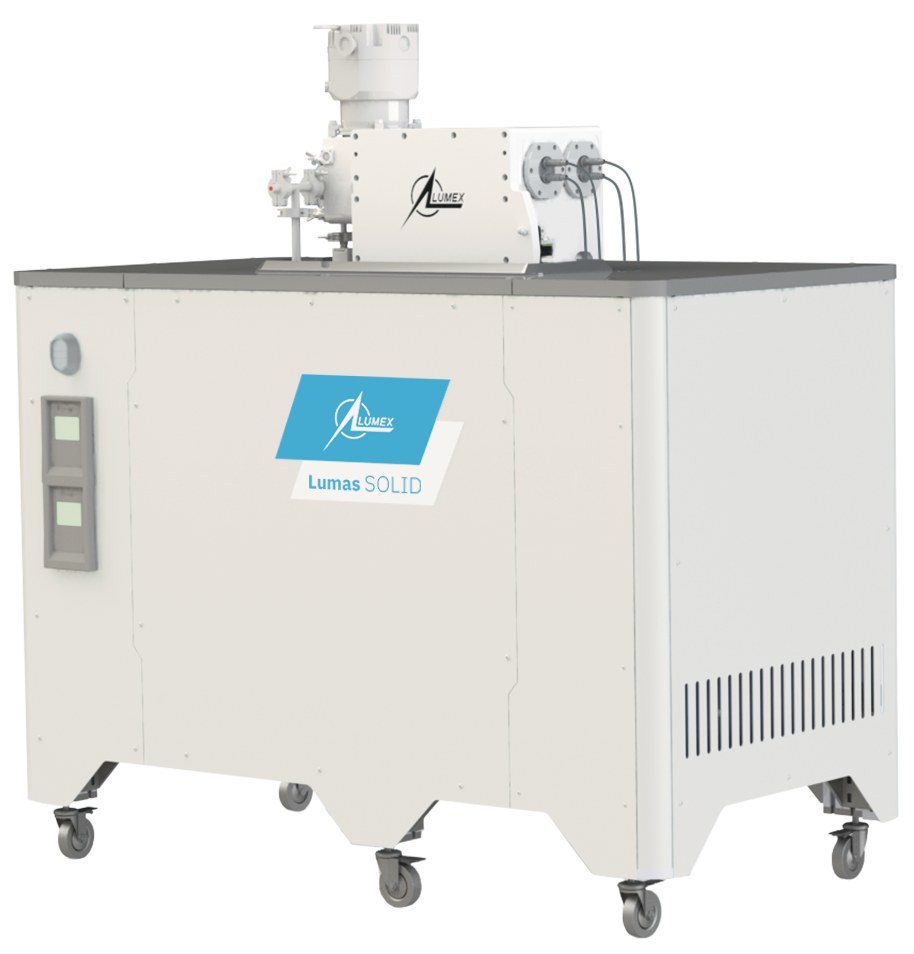
Mass spectrometer for the analysis of solid-phase samples "Lumas SOLID"
1 supp.
Technical specifications:
Method of ionization Plasma pulsed glow discharge
Discharge gas Argon, consumption less than 1 l/hour
Time-of-flight Mass Analyzer with mesh-free ion mirror
Resolution 4000
The number of simultaneously defined components is unlimited
Mass range 1-1000 m/z
Detection limits 1-100 ppb
Layer-by-layer resolution Up to 5 nm
Depth of analysis Up to 30 microns
The time for one analysis of a solid sample is 30 minutes (with the option of a revolver system – 3-5 minutes) Vacuum system 1 Booster pump and 2 TMN (240 l/sec)
Overall dimensions 1450×780×1550 mm
Lumeks
Saint Petersburg
Produced in: Saint Petersburg

Liquid analyzer "FLUORAT®-02-4M"
1 supp.
Technical specifications:
Limit of detection of the control substance (phenol) in water, mg/dm3, not more than 0.005
Measurement range of the mass concentration of the control substance (phenol) in water, mg / dm3 from 0.01 to 25
Measurement range of the directional transmission coefficient, % from 5 to 100
Limits of permissible absolute error of measurements of the directional transmission coefficient, % ±2 Warm-up time, min, not more than 30 Continuous operation time, h, not less than 8
Overall dimensions, mm, no more than 305x320x110
Weight, kg, not more than 6.5
AC power supply:
- AC power supply voltage, V
- frequency, Hz (220 ±22)
(50 ±1) Power consumption, V× A, no more than 36 Operating time for failure, h, no less than 2500
Lumeks
Saint Petersburg
Produced in: Saint Petersburg
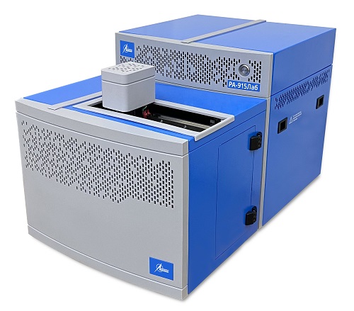
Laboratory mercury analyzer "RA-915Lab"
1 supp.
Technical specifications:
Measuring range 0.5–500 ng
Sample dispenser capacity 5000 mg / 2800 ml
Analysis time 1-5 min
Operating temperature range with software control 50-950 °C with software control
The capacity of the autosampler is 45 samples
Power supply 220 ± 22 V, 50 ± 1 Hz Dimensions (LxWxH), no more:
with autosampler
without autosampler
450x840x460 mm
450x490x460 mm
Weight, no more:
with autosampler
without autosampler
57 kg
40 kg
Lumeks
Saint Petersburg
Produced in: Saint Petersburg
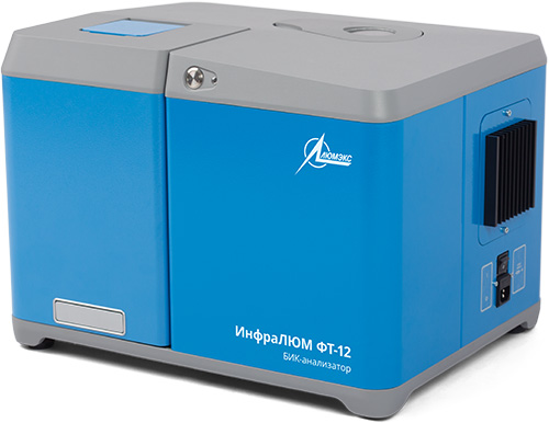
Infrared analyzer "InfraLUM® FT-12"
1 supp.
Technical specifications:
Measurement time, 80 seconds
Standard sample volume in a cuvette, 50 ml
Spectral range, cm-1 from 8700 to 13200
Spectral resolution, cm-1, no more than 10
The limit of the permissible value of the absolute error of the wave number scale, cm-1
±0,5
Analyzer warm-up time, min, no more than 30
Continuous operation time of the analyzer, h, at least 8
Overall dimensions, mm, no more than 530x450x380
Weight, kg, not more than 32
Power supply of analyzers from the AC network: AC power
supply voltage, V
frequency, Hz
(220 ±22)
(50 ±1)
Power consumption, V× A, not more than 110
Average time to failure, h, not less than 2500
Lumeks
Saint Petersburg
Produced in: Saint Petersburg
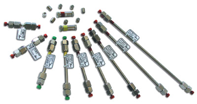
Chromatographic columns for HPLC
1 supp.
Variants of execution: - silica gel with grafted octadecyl groups (C18, RP, ODS) - for the variant of reversed-phase HPLC (OF HPLC);
- unmodified silica gel (SIL) – for normal-phase HPLC (NF HPLC).
Lumeks
Saint Petersburg
Produced in: Saint Petersburg
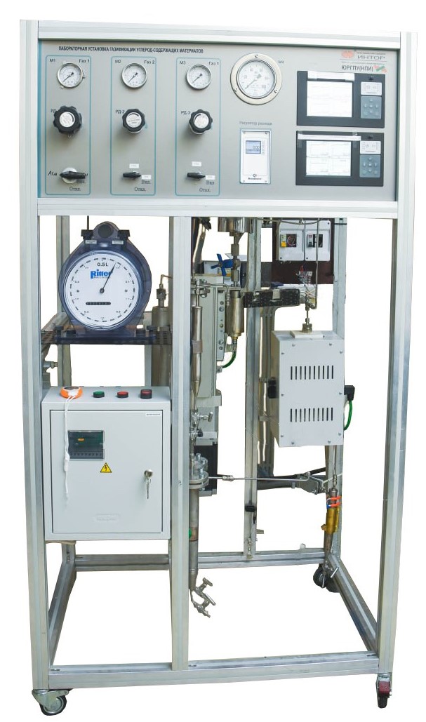
Laboratory hydrocracking/gasification unit
The laboratory unit is designed to study the catalytic and thermal processes of processing heavy petroleum raw materials.
The installation allows you to explore the following processes:
1. Hydrocracking
2. Thermal cracking
3. Gasification of water dispersions of coal, biomass, heavy oil residues.
The high-pressure liquid pump operates at temperatures up to 200°C, which makes it possible to supply high-viscosity components (fuel oil, tar, paraffin, ceresin, etc.) to the reactor.
The laboratory unit is manufactured in accordance with the technical requirements of customers so as to correspond to a wide range of technological parameters. The modular configuration of the unit allows you to change or upgrade it at any time for new tasks.
Main advantages:
1. The possibility of developing and supplying a reactor to meet customer requirements;
2. A wide range of accessories for the supply of liquids/solids;
3. Visual process control;
4. A system of control and regulation of technological parameters;
5. Convenience of loading and unloading of raw materials and reaction products;
6. The possibility of conducting long-term tests in continuous mode;
7. The possibility of upgrading the structure for new purposes;
8. Control and accurate reproduction.
YURGPU(NPI) FGBOU VO "YURGPU(NPI) IMENI M.I.PLATOVA"
Novocherkassk
Produced in: Rostov region, Novocherkassk
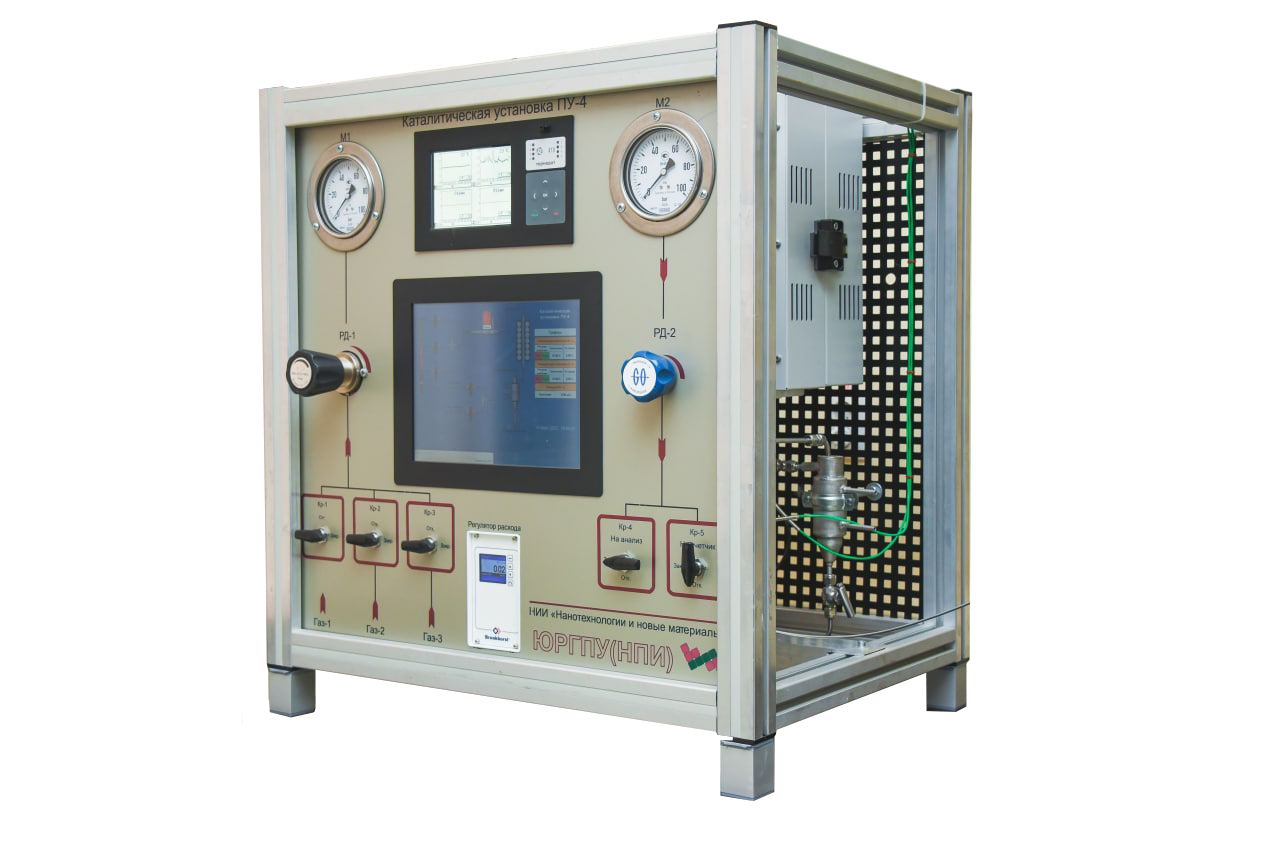
PU Desktop laboratory catalytic unit
The PU desktop laboratory unit is an automated installation based on a mini–reactor with a fixed layer that has a volume of up to 1.5 cm3. The PU desktop laboratory unit is designed to perform kinetic studies, evaluate the properties of catalysts, model catalytic processes, test the stability of catalysts and sorbents.
For maximum compliance with the customer's requests, the installation has a modular design with the possibility of adding new options.
Main advantages:
1. Compactness;
2. Real-time parameter monitoring;
3. Easy maintenance;
4. Operation safety;
5. User-friendly interface.
Applied tasks
1. Hydrogenation/dehydrogenation processes of hydrocarbons;
2. Fischer-Tropsch synthesis;
3. Catalytic cracking and isomerization;
4. Reforming of natural gases;
5. Hydrogenation processes;
6. Catalytic oxidation;
7. Hydrotreating processes.
Basic equipment
1. Gas supply unit
2. Reactor unit
3. Separation unit
4. Sampling unit
5. Unit for measuring the volume of the outgoing gas
6. Control unit
YURGPU(NPI) FGBOU VO "YURGPU(NPI) IMENI M.I.PLATOVA"
Novocherkassk
Produced in: Rostov region, Novocherkassk
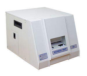
Capillary electrophoresis systems "KAPEL®-104T"
1 supp.
Technical specifications:
The working wavelength of detection, nm 254 The range of variation of the operating voltage on the capillary, kV from 1 to 25
The detection limit of benzoic acid (with positive polarity of the high-voltage unit) at a signal-to-noise ratio of 3:1, mcg/ cm3, not more than 0.8
The limit of detection of chloride ions (with a negative polarity of the high-voltage unit) at a signal-to-noise ratio of 3:1, micrograms / cm3, not more than 0.5
The limit of the permissible relative mean square deviation (SKO) of the output signal over the peak area, %5
The limit of the permissible relative mean square deviation (SKO) of the output signal for 8 hours of operation, % 6.5
Operating mode setting time, min, no more than 30
Power supply of systems from the AC network with voltage, V; frequency, Hz.
220 ±22 50 ±1
Power consumption consumed by the system, In ×A, no more: 150
Overall dimensions (LXC), mm, no more
420x460x360
Weight, kg, not more than 25
Lumeks
Saint Petersburg
Produced in: Saint Petersburg
